

Flexible, Affordable Electronics Education
Online courses and webinars for the printed circuit engineering community.
Current Workshops
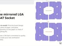
Hair-Raising Footprint Horror Stories – and How to Avoid Them
When creating libraries, standards are crucial for maintaining consistency, accuracy, and reliability. Yet, even with rigid standards in place, mistakes inevitably creep into such a detail-oriented... [more]
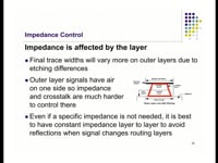
Routing Digital Boards to Avoid Problems
There are many ways to route a PCB, some much more effective for signals than others. The first design rule is that the board must work properly, so it is important to have a plan that addresses... [more]
The Case for Split Ground Planes
Some experts say you should never use a split ground plane. Others say you should use a split ground plane to control noise. When is the right time to split a ground plane? We will explore the... [more]
PC Board Grounding to Control Noise, EMI and Signal Integrity
When time-varying (AC) signals travel in the transmission lines of a board, state-changing electric and magnetic fields are present. These fields, when not controlled, are the source of noise and... [more]
Topics


